On this page
Light is useful for moving data quickly, but a laser can be unsettled by light that reflects back into it. Optical isolators normally block that return path. A Waseda-led research team has demonstrated another approach: design the wavelength-dependent behavior of several photonic components together so the transmitter remains stable without a separate isolator.
How the chip controls feedback
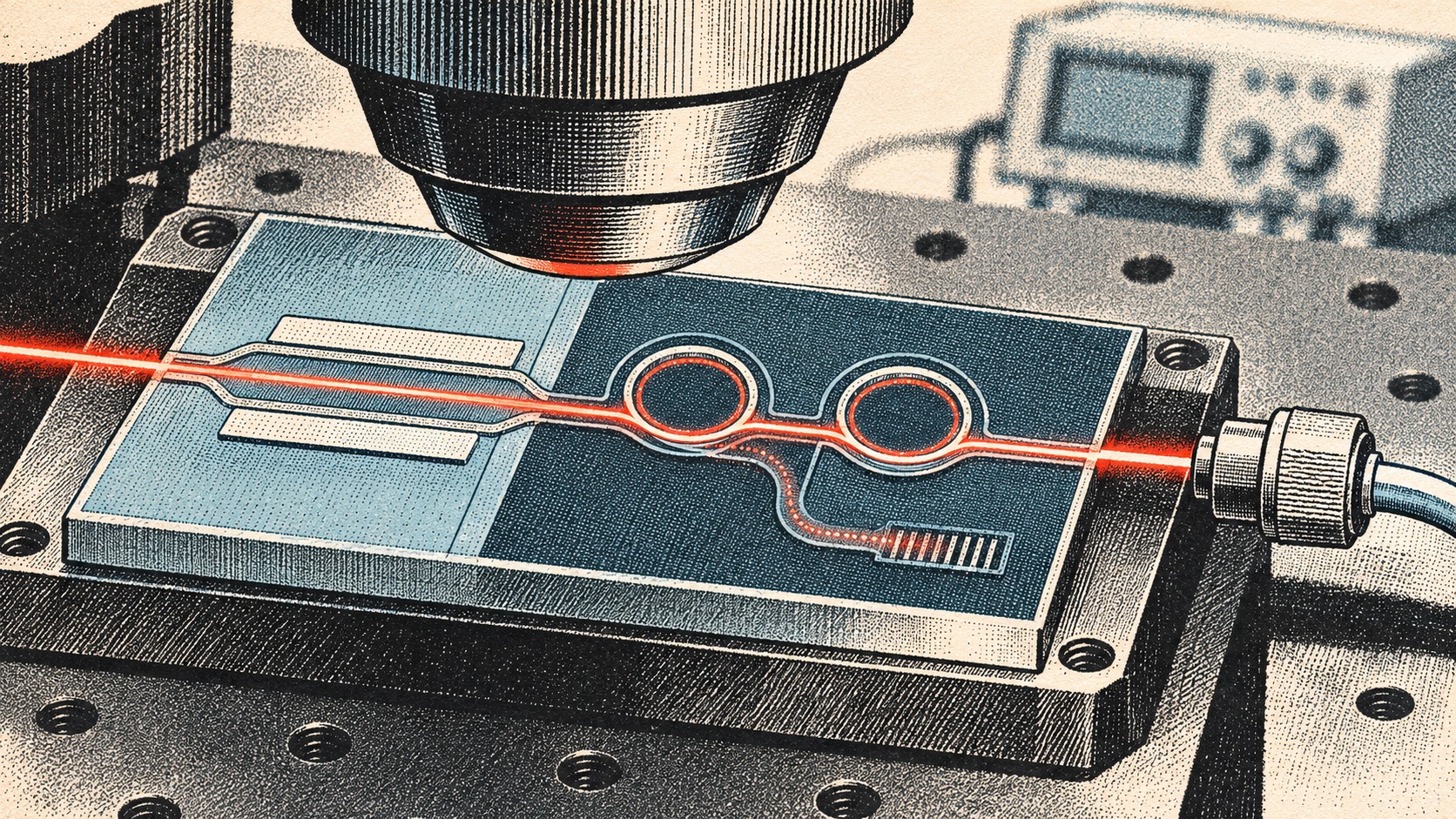
The transmitter combines a wavelength-tunable external-cavity laser with a silicon-nitride photonic circuit and a thin-film lithium-niobate modulator. Two ring resonators form a Vernier filter that selects the laser’s wavelength. The modulator encodes data onto the light using an asymmetric Mach–Zehnder interferometer. Its wavelength-dependent transmission is designed alongside the filter so reflected light is less destabilizing to the laser. [1] [2]
The team reported stable operation over an approximately 67-nanometer range without active temperature control and demonstrated transmission at 180 Gbit/s. The researchers identify 180 Gbit/s as the highest rate tested in the experiment, not a measured ceiling for the design. Their paper appeared in the Journal of Lightwave Technology in October 2026. [1] [2]
The advance is in component integration and feedback management. Conventional isolators are useful because they prevent backward-traveling light from re-entering a laser. Eliminating one could simplify a photonic package, but only if the integrated design stays stable across the operating conditions the product will face. The paper’s result is one proof point for a particular chip architecture, not a general replacement for isolators in optical systems.
A data-center implication, with caveats
The researchers point to high-capacity links between data centers as a possible application. That is a reasonable direction: AI systems and cloud services move large volumes of information between machines, and photonic integration can bring lasers, filters, and modulators closer together. The device’s 67-nanometer wavelength range may also be relevant to wavelength-division multiplexing, where several optical channels share one fiber. [1]
But one transmitter experiment does not show that a full data-center link is ready. A deployment would also need to establish error rates, optical power budget, fiber reach, channel spacing, thermal stability over time, packaging tolerances, manufacturing yield, and compatibility with receiver and network components. None of those system-level metrics can be inferred from a headline data rate alone.
There is also a difference between transmission speed and useful system capacity. The paper’s 180 Gbit/s result describes the demonstrated data transmission in its setup. A commercial link must retain acceptable error performance over its target distance and environment while meeting power, cost, and maintenance requirements. Until those measurements are published, footprint reduction and lower system cost remain possible outcomes rather than demonstrated benefits.
What would make the result deployable
The most useful follow-up would compare the isolator-free design with an otherwise similar transmitter that includes an isolator. The comparison should report insertion loss, laser stability under controlled reflections, data error rates, temperature range, optical power, and repeatability across multiple fabricated devices. Reliability testing would show whether the resonator and modulator alignment survives normal manufacturing variation and long operation.
For infrastructure teams, the near-term implication is to watch the component roadmap, not plan a migration around one lab result. The design is an example of co-design across photonic materials and functions: a silicon-nitride filter and a lithium-niobate modulator work together to solve a feedback problem. Our related coverage of optical I/O for GPU clusters and the AI-optics supplier landscape examines adjacent layers of the interconnect stack.
Frequently asked questions
What did Waseda’s optical transmitter demonstrate?
The team reported stable laser operation across about 67 nanometers and data transmission at 180 Gbit/s in a laboratory experiment. The tested data rate was the highest examined in that study, not a demonstrated production maximum.
Why does an optical transmitter use an isolator?
An optical isolator blocks reflected light from traveling back into a laser, where feedback can destabilize its output. The Waseda design instead co-designs wavelength-dependent responses in its resonators and modulator to manage that feedback.
Is the isolator-free transmitter commercially available?
The announcement describes a research prototype and a possible path to more compact photonic integrated circuits. It does not announce a commercial product or production deployment.
Sources & further reading
Keep reading

Rice’s Heat Q-Switch Stores a Steady Stream for a Brief Burst
Rice engineers built a fluidic device that stores heat as water flows, then releases a thermal pulse. The extra power comes from stored energy.

JWST’s New Exoplanet Image Shows What Better Glare Models Can Reveal
FLIP uses a physics-based model to subtract starlight from JWST images, uncovering a faint planet while exposing the limits of computational recovery.

Google’s Gen AI Python SDK 3.0 Changes Three Defaults. Check Before You Upgrade
Google Gen AI Python SDK 3.0 changes the API default, HTTP client and one result type. Here is what Gemini developers should check before upgrading.
/* Comments */
Comments are offline right now — we reconnect automatically, nothing is lost.